Bridging Innovation and Excellence in Advanced Manufacturing Solutions
a close up of a printed circuit board

About Henger Plasma

We deliver top-quality plasma machine solutions for electronics manufacturing.

A bright blue plasma arc extends from the left to the right of the image, connecting two electrical nodes, possibly a Tesla coil or similar device. The plasma is luminous and appears to be sizzling with electrical energy.
Industry Leadership

HENGER’s plasma etching and cleaning equipment is widely adopted by leading PCB manufacturers, offering high-performance solutions that optimize efficiency, precision, and sustainability in modern electronics production.

man in white dress shirt sitting on black office rolling chair
Strong R&D capabilities

With strong R&D capabilities, patented designs, and automation-driven plasma systems, HENGER ensures efficiency, precision, and reliability, keeping manufacturers at the forefront of modern electronics production.

A person is assembling or inspecting a green printed circuit board (PCB) with various components mounted on it. The setting appears to be an industrial or technical environment.
A close-up view of a green printed circuit board (PCB) featuring a variety of silver and black electronic components. There are several connections, solder points, and visible traces along with some text labeling on the surface. The board appears to be resting on a slightly worn, off-white workbench with some signs of use around it.
Continues to Innovate

Meeting evolving needs through dedicated service and innovation.

Industry Expertise

Representing leading manufacturers to serve customers across North America effectively.

Innovative Plasma Solutions

Expert representation for PCB and electronics industries across North America, fostering growth and excellence.

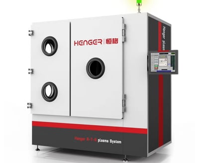
Roll-to-roll Plasma Desmear Etching Equipment PL06-300

Designed for FPC hole degluing, surface cleaning, PI surface roughening and cleaning, electronic material surface roughening and cleaning, Coverlay surface roughening and cleaning, and flexible material surface cleaning.

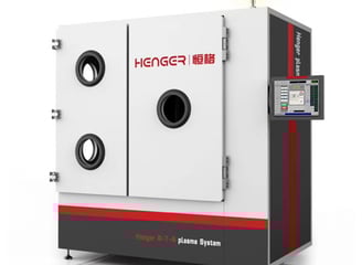
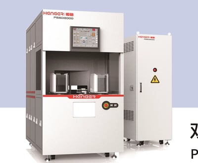
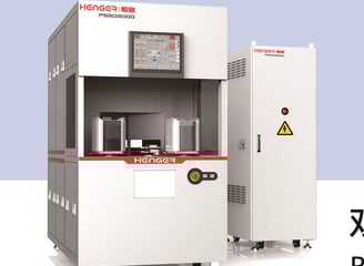
PSSD2000 (PR Ashing)

Designed for chip-level applications. It specializes in removing photoresist (PR) layers, offering advanced features for efficient and precise ashing processes, ensuring high-quality results for delicate chip-level operations.

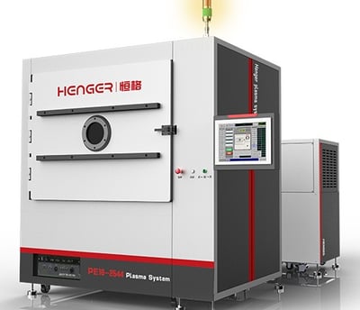
Vertical Plasma Cleaning and Etching Equipment PE06-2544

We provide cutting-edge plasma machine solutions tailored for the PCB and semiconductor industries.

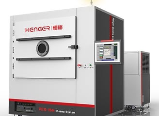
Vertical Plasma Cleaning and Etching Equipment PE08-2544

Vertical Plasma Cleaning and Etching Equipment PE16-2544

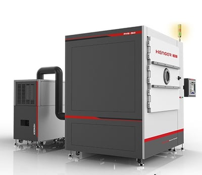
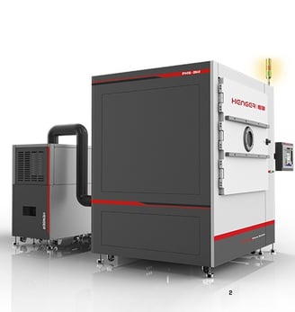
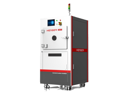
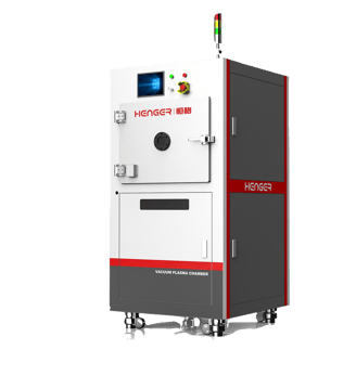
Horizontal Plasma PH16-2842
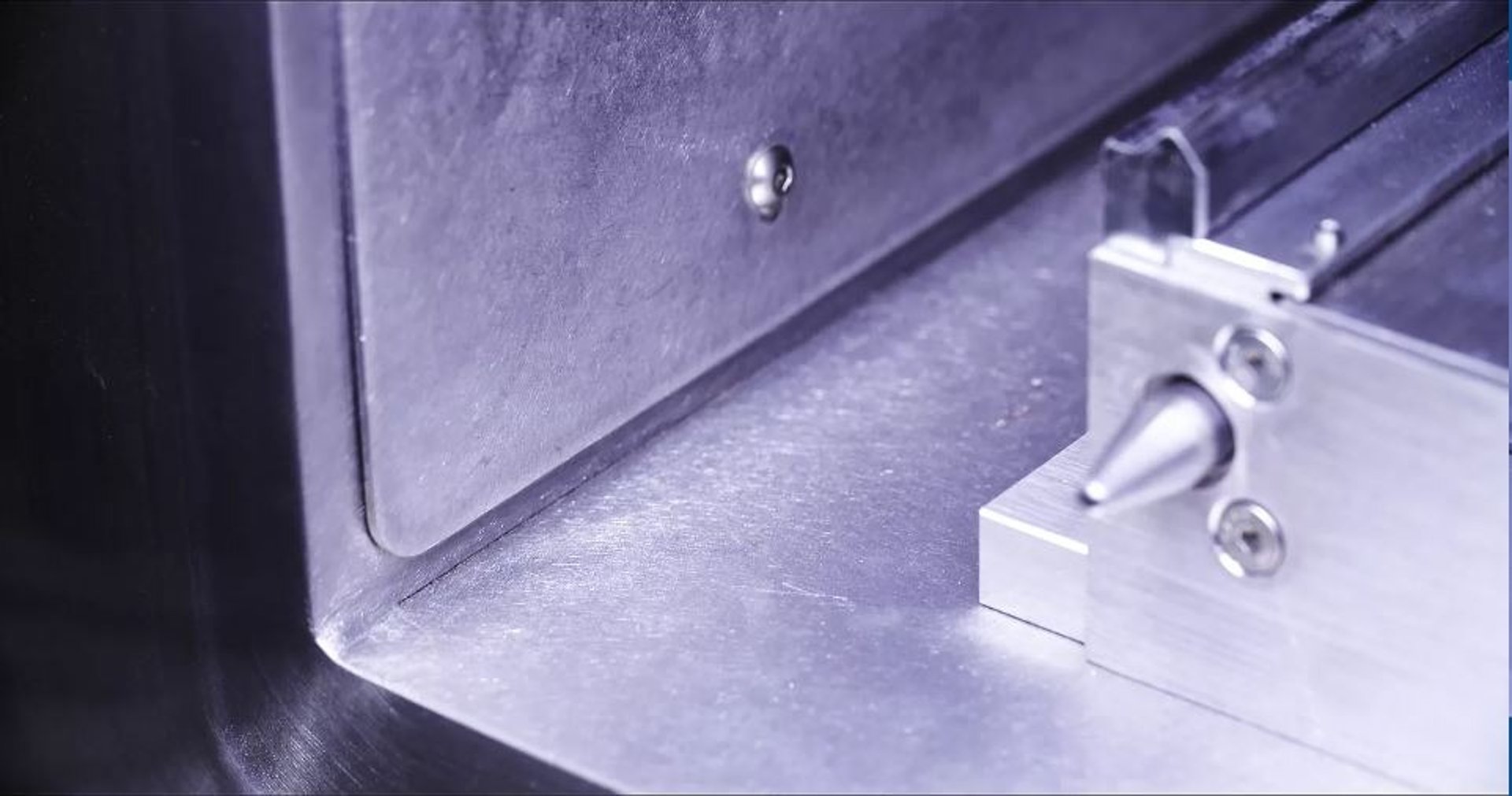
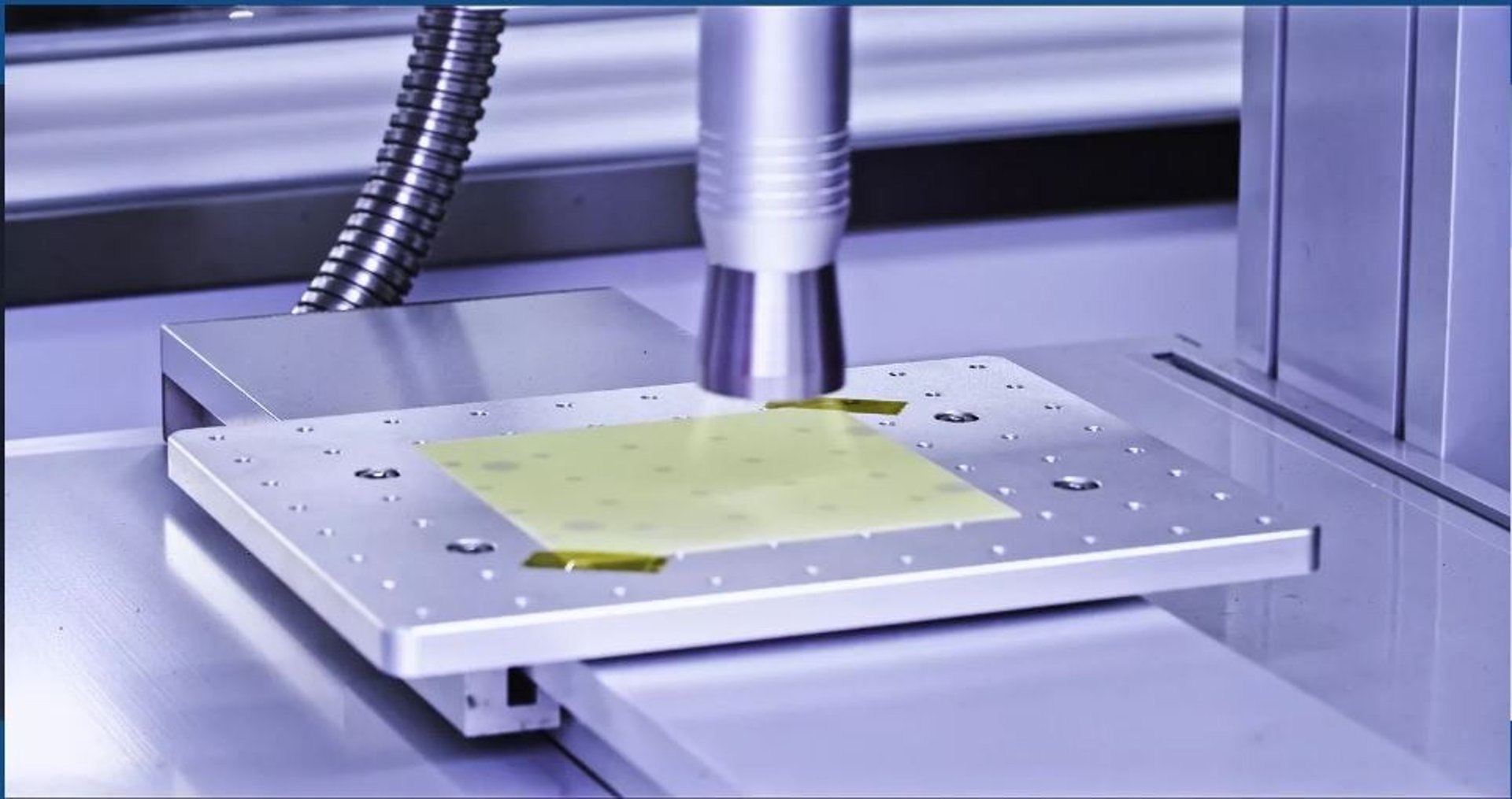
Innovative Solutions

We provide advanced plasma machine solutions for electronics industries.

A close-up view of an electronic circuit board illuminated with a red LED light. Twisted wires are connected to the circuit board, and the background is bathed in blue lighting. There is a honeycomb-like pattern visible on the right side, possibly part of a protective casing.
Cutting-Edge Technology

Bridging technology and manufacturers for optimal growth and service.

A precision laser cutting machine appears in a workspace, with a laser head marked 'Opt Lasers' actively cutting or engraving material. The machine is mounted on a linear rail system, and the surrounding area is dark, highlighting the blue light emitted by the laser.
A laboratory apparatus setup featuring a white machine with two nozzles and tubes on top, a blue control unit with digital display and buttons, and a white rectangular box with slotted openings.
A machine is actively engaged in cutting or engraving a metallic surface with precision. The left side of the image shows a control panel with various buttons, one of which is red, and two indicator lights that are illuminated. The metallic surface has visible cut marks and circular shapes, indicating ongoing or completed cutting processes. The cutting tool emits a bright orange light as it makes contact with the metal.
Trusted Representation

Representing PCB and electronic manufacturers across North America effectively.

Gallery

A machine or industrial device with metallic components, including a cylindrical part and wiring, is positioned near a pink material with circular cutouts on a gray surface.
A close-up view of a printed circuit board featuring various electronic components such as resistors, capacitors, and connectors. The board has visible green solder mask and orange, black, and beige components mounted on it, with white markings for labeling.
A close-up view of a red printed circuit board with various electronic components. The board features a rectangular black microchip with multiple pins, several resistors, capacitors, LEDs, and a cylindrical battery holder. A barcode is visible on one of the components, and there are intricate traces and connections soldered onto the board.
A close-up view of a microchip on a circuit board being worked on with precision instruments. The scene is illuminated, highlighting the intricate electronic components and the fine details of the circuit.
A close-up view of electronic components on a circuit board, including capacitors, inductors, and semiconductor chips. The components are densely packed, with visible QR codes on some of the parts. The circuit board is part of a larger electronic device with a metallic enclosure.
A 3D-rendered image of a green circuit board depicting various electronic components, including a central purple chip with a symbol, multiple smaller chips, capacitors, and resistors. The board features intricate gold circuitry pathways.

Showcasing innovative plasma solutions for electronics and manufacturing.