Bridging Innovation and Excellence in Advanced Manufacturing Solutions
Plasma For Semiconductor
Expert representation for PCB and electronics industries across North America, fostering growth and excellence.
Henger Microwave Plasma De-gluing Machine PSSD2000 (PR Ashing) – Chip-Level
The semiconductor industry demands precision in deposition, removal, patterning, and electrical property modifications as devices continue to shrink while increasing in speed and efficiency. Meeting these evolving requirements presents challenges such as ultra-thin layers, reduced critical dimensions, novel materials, and complex 3D architectures.
To address these needs, GaN solid-state microwave technologies provide high-efficiency solutions for semiconductor processes, including chemical vapor deposition (CVD), annealing, and plasma-assisted etching. These advanced systems enhance precision, ensure uniform heating, and accelerate throughput, allowing manufacturers to optimize yield and productivity
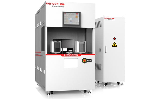
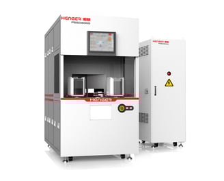
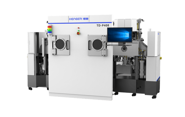
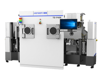
Henger 12-inch Wafer Microwave Plasma De-gluing and Surface Treatment System
Core Advantages:
Low Damage & High Efficiency: High etching rate and uniformity ensure process stability.
Wide Compatibility: Supports 8-inch and 12-inch wafers, adaptable to highly warped substrates and various materials.
Enhanced Hydrophilicity: Optimized surface treatment improves the quality of subsequent processes.
Modular Design: Fully automated parallel operation ensures stable performance and high productivity.
Cost-Effective Ownership: Provides customers with high-value solutions at competitive costs.
High-Capacity Design: Twin-chamber structure for dual-wafer processing.
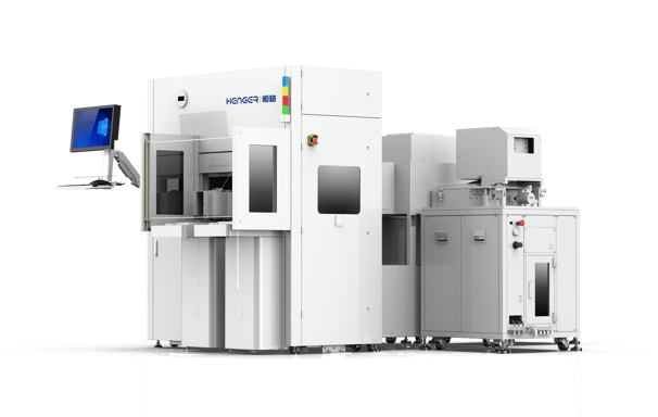
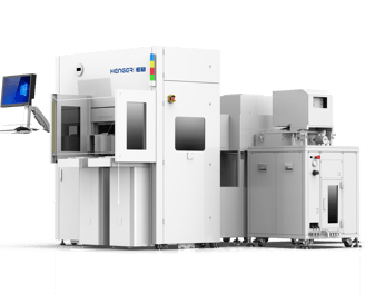
Sic Etching System
Applicable to 6-8 inch compound etching (SiC, GaN, SOl wafer), TGV, TCV and other processes. Different configurations can be compatible with TSV, DRiE and other processes.
Core Advantages:
High etching rate, high output, excellent uniformity.
Adapt to warped products, easy maintenance, low operating costs & small footprint
Process performance:
Silicon carbide etching rate:>1.3um/min Silicon etching rate:>10um/min
Silicon etching depth:>400um Good uniformity:≤3%
Good particle control:<50 ea Smooth sidewall morphology without corners, flat bottom
Selectivity (SiC to Si02):>14:1
Trusted By Major Businesses Worldwide
Unwavering Commitment To Excellence And Quality