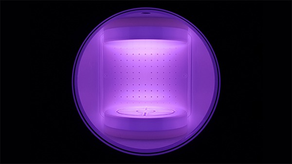
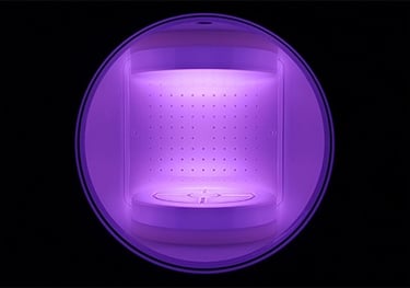
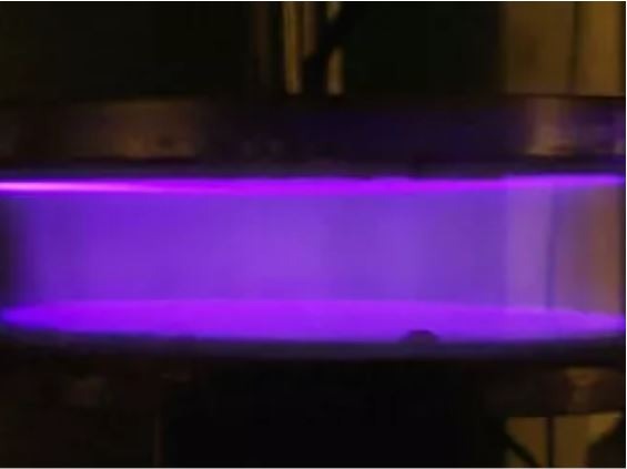
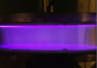
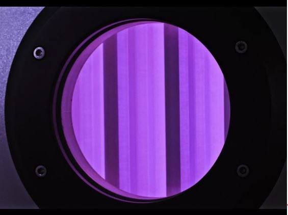
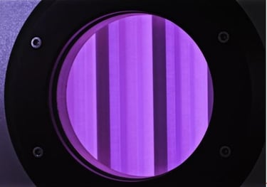
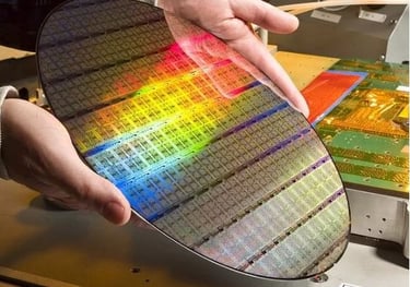
Plasma Technology & Benefits
Microfine Cleaning
Removes even the smallest dust particles from substrates, ensuring optimal surface conditions for further processing
Superior Adhesion & Etching
Creates chemically reactive surfaces for improved bonding in coatings, films, and semiconductor applications.
Surface activation
A micro/nanofabrication technique that leverages partially ionized gas to selectively modify material surfaces. Enables precise pattern transfer and surface preparation.
Photoresist Removal
Removes photoresist via ion bombardment and chemical reactions, providing precise, residue-free cleaning.


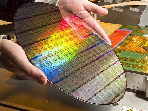
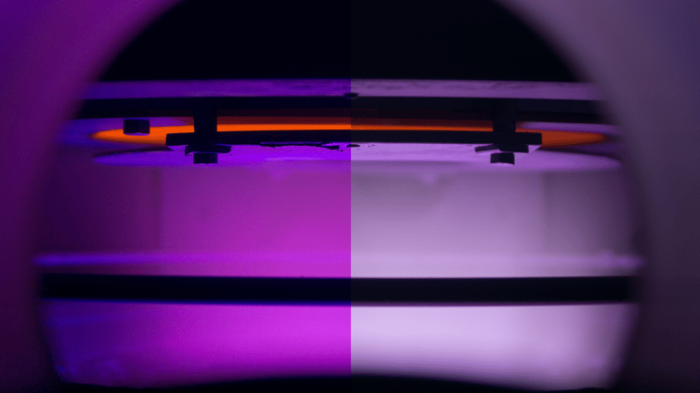
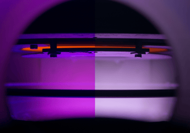
Dry Etching
Plasma-based techniques (e.g., RIE, ICP, DRIE) for material removal without liquid chemicals. It combines anisotropic physical sputtering and chemical reactions for high-precision patterning.
Plasma-Enhanced Chemical Vapor Deposition (PECVD)
PECVD enables high-quality thin-film deposition using plasma-activated precursors at low temperatures (<400°C), making it ideal for heat-sensitive substrates.