
Plasma Solutions Excellence By Visnex
Exclusive representation for top-tier plasma solutions tailored for manufacturers' needs.
Expert Guidance & Support
As the exclusive representative, we provide specialized expertise, helping customers optimize plasma technology for PCB and semiconductor applications.
Top-Tier Solutions
Access to industry-leading plasma innovations, helping manufacturers stay ahead in efficiency, precision, and sustainability.
Exclusive Access
Providing manufacturers with top-tier plasma equipment without intermediaries, ensuring authentic and high-performance solutions.
Priority Service & Customization
Customers benefit from tailored solutions, faster response times, and dedicated technical support.
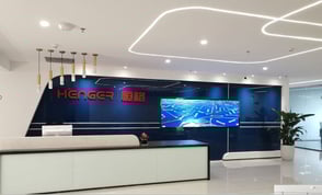
Microelectronic Equipment Co. Ltd.
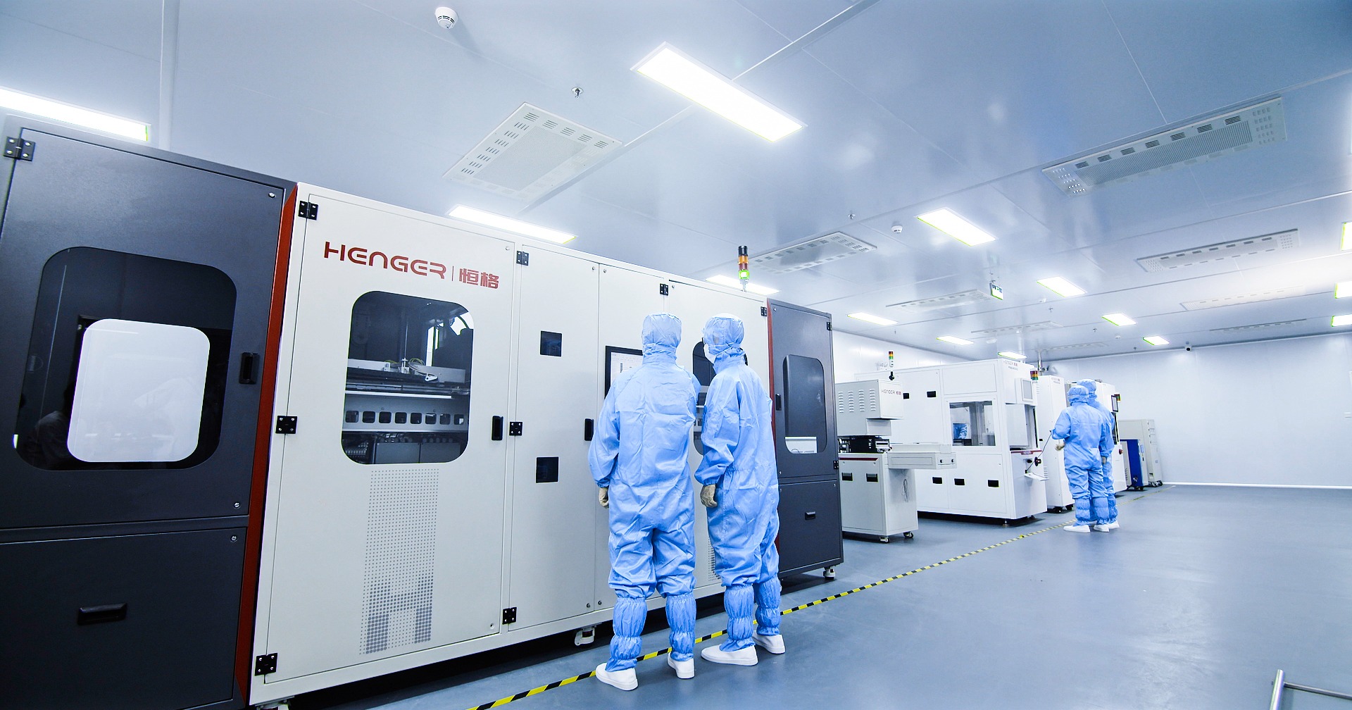
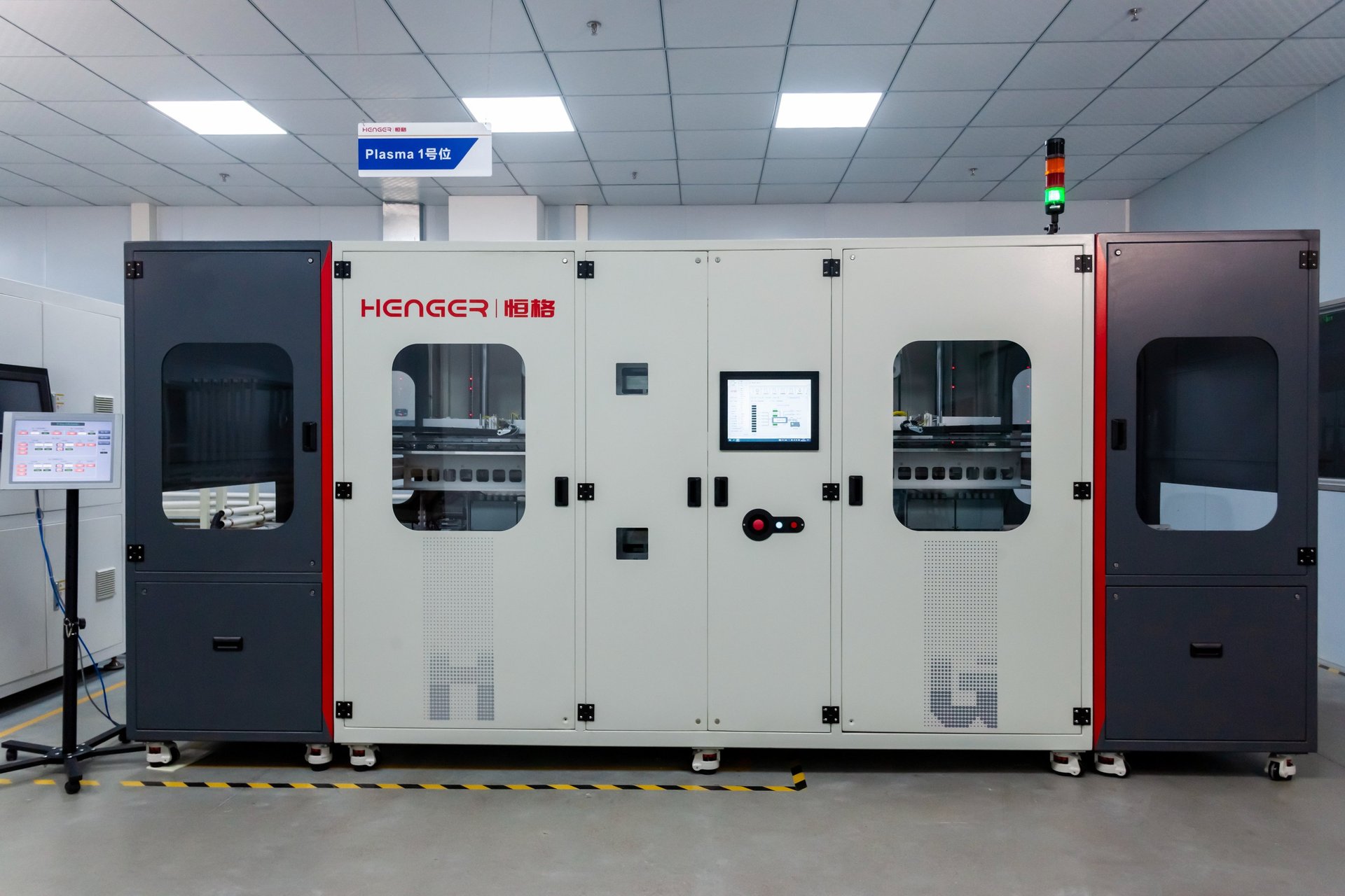
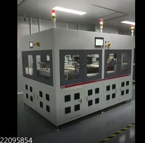
HENGER specializes in advanced plasma etching and cleaning equipment, with state-of-the-art facilities in Zhuhai and Dongguan. Backed by a highly skilled technical team with over a decade of expertise, Henger ensures exceptional quality and a 99%+ first-pass yield rate. Henger plasma are trusted by top tier PCB manufactuers around the globe.
About Henger Plasma
We deliver top-quality plasma machine solutions for electronics manufacturing.


Industry Leadership
HENGER’s plasma etching and cleaning equipment is widely adopted by leading PCB manufacturers, offering high-performance solutions that optimize efficiency, precision, and sustainability in modern electronics production.
Strong R&D capabilities
With strong R&D capabilities, patented designs, and automation-driven plasma systems, HENGER ensures efficiency, precision, and reliability, keeping manufacturers at the forefront of modern electronics production.


Global Presence
Currently 12 Service centers across China and East Asia. Entrusted Visnex as its exclusive representative in North American, connecting manufacturers with cutting-edge plasma equipment to drive innovation, efficiency, and industry advancement.
Industry Impact
HENGER’s plasma machines are widely adopted by 60% of the top 20 PCB manufacturers worldwide, recognized for their cutting-edge technology, precision, and efficiency in high-performance circuit board production
→
→
→
→
Our mission
At HENGER, we are committed to advancing technology, shaping the future, and creating lasting value for our customers. Our mission is to drive innovation in plasma equipment, delivering cutting-edge solutions that revolutionize PCB and semiconductor manufacturing.
Our vision
We envision a future where plasma technology reshapes the PCB and semiconductor industries, driving higher efficiency, precision, and sustainability. Through continuous innovation and strong R&D, we aim to lead the industry with cutting-edge plasma solutions, bridging technology providers with manufacturers for mutual growth and long-term success
Learn More About Henger Plasma
Discover the technological advantages that set HENGER apart in plasma etching and cleaning solutions.

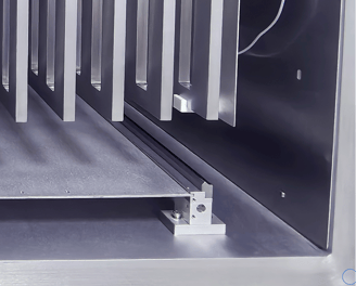
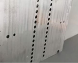
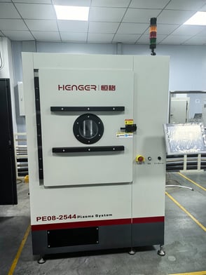
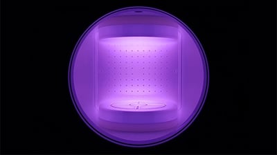
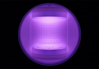
Seamless Design Chamber
Aerospace-grade aluminum chambers feature seamless welding for durability and precision. With a vacuum leakage rate below 20 mTorr/min, the system ensures optimal uniformity.
Intergrated Design Electrode
Integrated electrode forming technology with seamless welding, ensuring high durability and precision and a 20% higher heating efficiency.
Independent Tempreture Control
Independent cooling system for electrodes, RF power supply, and vacuum pump, ensuring operational stability and significantly extending equipment lifespan.
Advanced Cooling & Gas Protection
Integrates helium-oxygen software protection, ensuring precise gas flow control and system stability. The gas flow & pressure alarm system provides real-time monitoring, preventing fluctuations and optimizing processing efficiency.
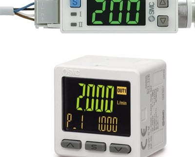
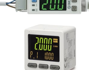
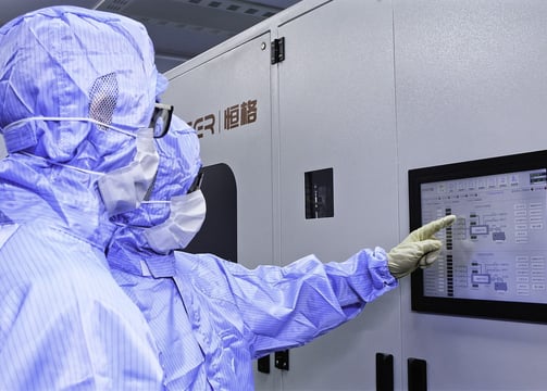
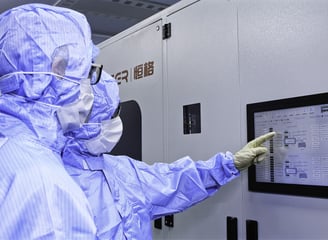
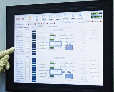
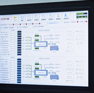
Remote Real Time Control
PLC human-machine interface software allows real-time data recording, permanent storage, and secure user management.

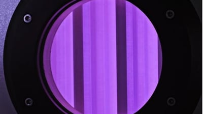
Removable Chamber Panel
Removable internal panels within the chamber, providing enhanced protection, easy cleaning, and increased efficiency. This design ensures uniform plasma erosion,
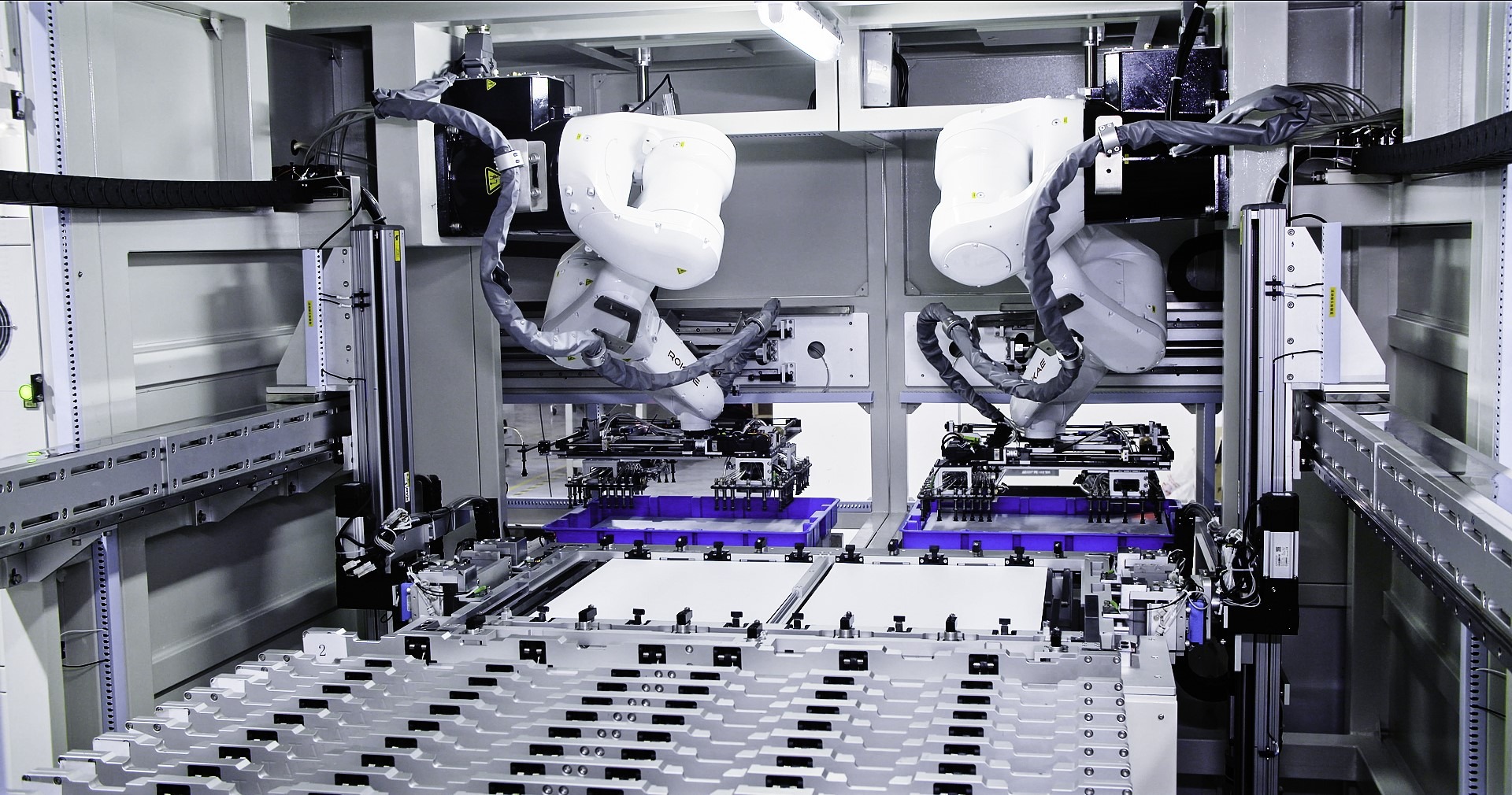
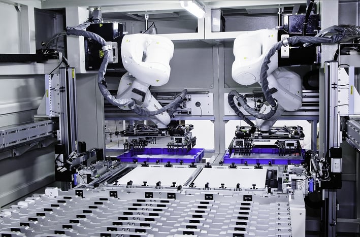
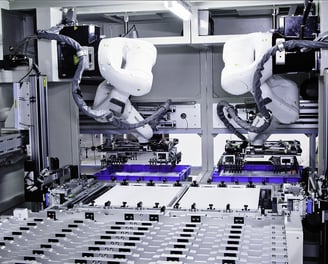
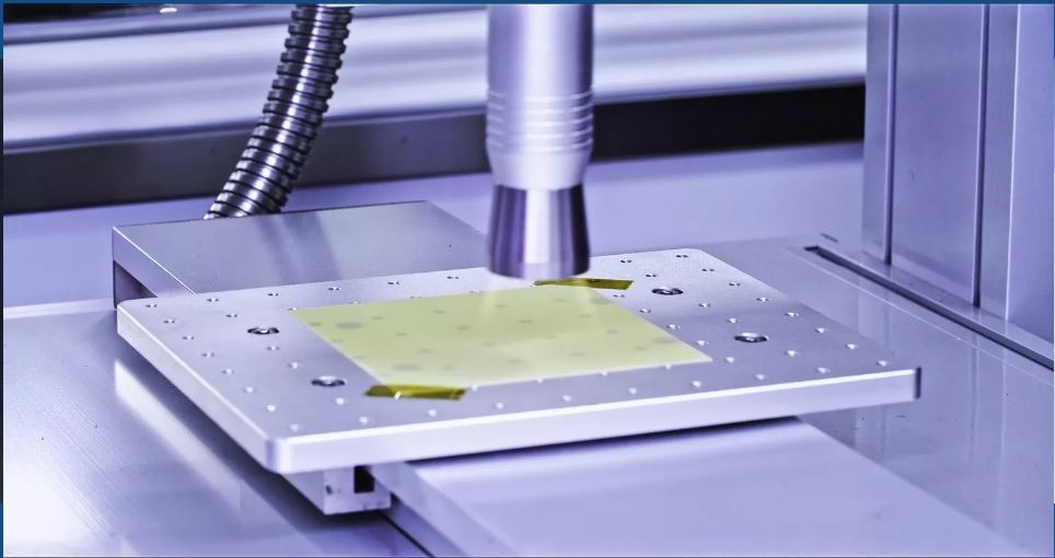
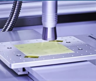
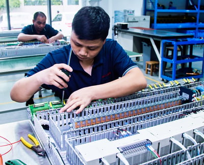
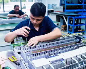
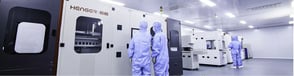
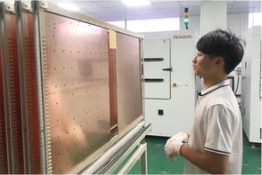
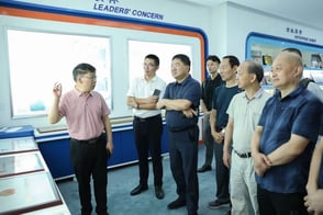
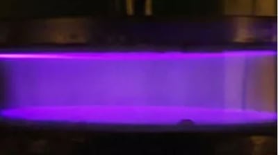
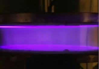
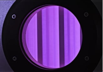
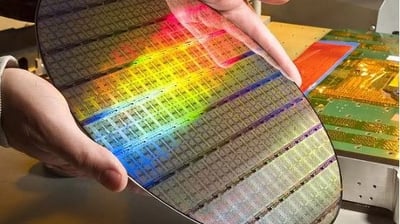
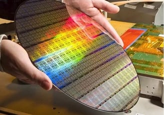
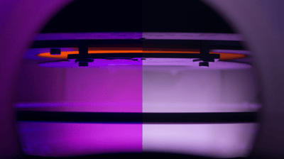
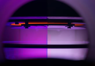
Beyond the Lab: Plasma in Action
A Behind-the-Scenes Look at Our Plasma Technology: From Research to Manufacturing and Customer Collaboration

Plasma Technology & Benefits
Microfine Cleaning
Removes even the smallest dust particles from substrates, ensuring optimal surface conditions for further processing
Superior Adhesion & Etching
Creates chemically reactive surfaces for improved bonding in coatings, films, and semiconductor applications.
Surface activation
A micro/nanofabrication technique that leverages partially ionized gas to selectively modify material surfaces. Enables precise pattern transfer and surface preparation.
Photoresist Removal
Removes photoresist via ion bombardment and chemical reactions, providing precise, residue-free cleaning.


Dry Etching
Plasma-based techniques (e.g., RIE, ICP, DRIE) for material removal without liquid chemicals. It combines anisotropic physical sputtering and chemical reactions for high-precision patterning.
Plasma-Enhanced Chemical Vapor Deposition (PECVD)
PECVD enables high-quality thin-film deposition using plasma-activated precursors at low temperatures (<400°C), making it ideal for heat-sensitive substrates.